
By Industry
Semiconductor & Electronics
Advanced packaging, display bonding and PCB protection — UV curing next to die that cannot take heat.
The problem
UV curing in Semiconductor & Electronics
Semiconductor and electronics assembly keeps asking the same question: how do you cure an adhesive fast, next to a die, a sensor or a flex circuit that will not tolerate the heat of a thermal cure. UV LED answers it — the energy goes into the photoinitiator, not into the substrate.
From wafer-level underfill dams and advanced packaging to OCA display lamination, conformal coating and component staking, ETIA matches the source to the geometry: spot heads for point bonds, small-area arrays for sub-assemblies, and wide arrays for panel and web lines.
Processes we solve
Advanced packaging & underfill dams
Precise, localised cures that fix dam geometry without thermally stressing the die.
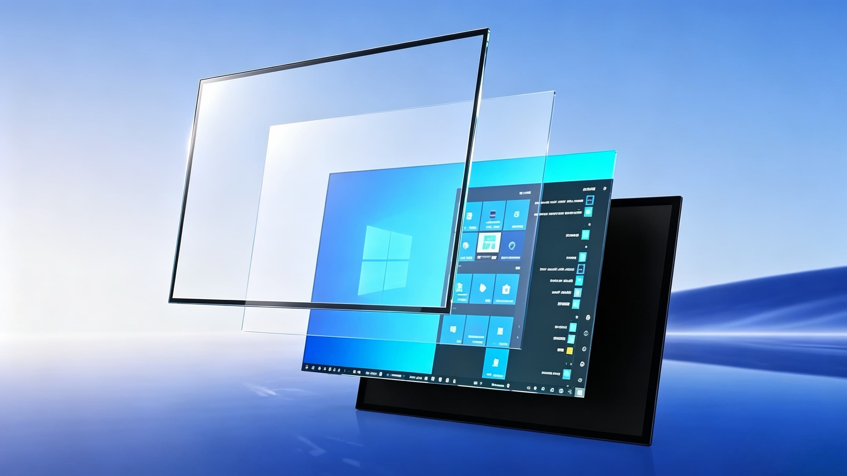
Display OCA & edge sealing
Uniform large-area dose for optically clear adhesive lamination and OLED edge seals.
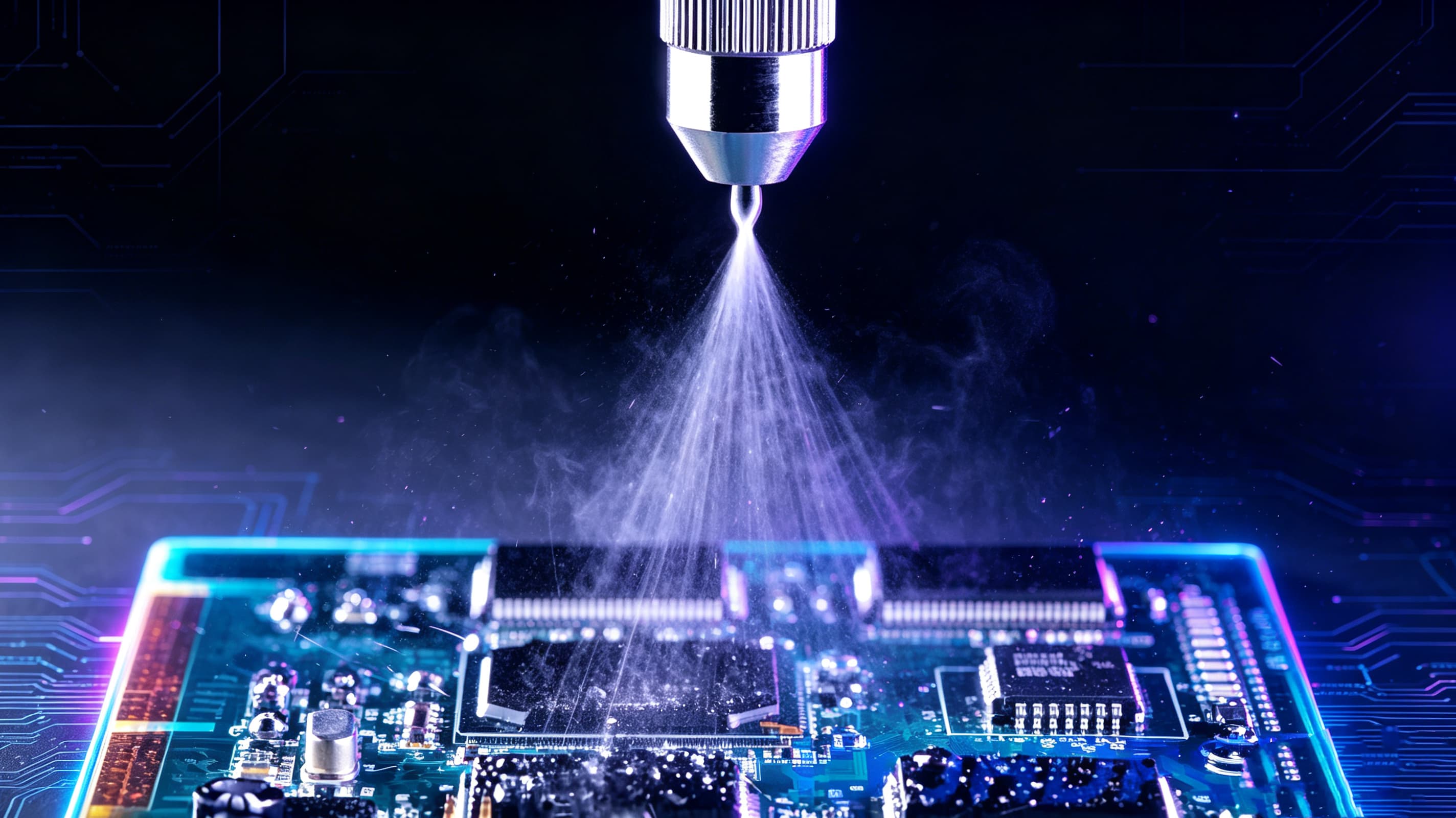
PCB conformal coating
Seconds-scale cure of protective coatings, in line, with no oven footprint.
Component staking & wire tacking
Vibration-proof anchoring of tall components and loose wires on populated boards.
Potting & encapsulation
UV-cure encapsulants that protect assemblies without long thermal dwell times.
Recommended technologies
Application notes
All applications
Photonics & Advanced Packaging
UV Curing for Advanced Semiconductor Packaging
UV curing solutions for chiplet bonding, underfill cure, photonic interconnect bonding, and UV dicing tape release.
Read application →
Electronics & PCB Assembly
UV LED Curing for Display Module OCA Bonding
Controlled low-heat UV LED curing for optically clear adhesive bonding in display module assembly.
Read application →

Electronics & PCB Assembly
UV LED Curing for OLED Panel Edge Sealing
Low-heat UV LED curing for moisture-sensitive OLED edge sealing and display encapsulation.
Read application →
Electronics & PCB Assembly
UV LED Curing for PCB Conformal Coating
Fast UV LED curing for PCB protection in electronics and automotive assembly.
Read application →
Bring us the joint that won't hold.
Our engineers work the problem with you — adhesive, geometry, dose and takt — and specify the system that fits your line.